Design challenge

Embedding on-chip memory allows the SoC designer to try and scale the memory wall, by customising for bandwidth, word length, etc. This approach increases bandwidth, hides latency and lowers total system power consumption by reducing off-chip memory accesses.

But implementing on-chip L3/LLC cache and on-chip main memory is also challenged by the scaling, power and cost walls.

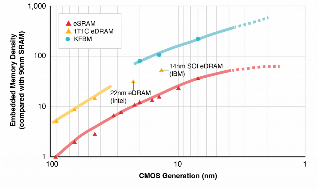
Embedded SRAM (eSRAM) does not scale as easily as logic, as transistor performance variation increases, making the SRAM unstable. Leakage current also increases, and immunity to soft errors is compromised. In fact, SRAM scaling has stalled below 7nm, threatening the opportunity to increase
SRAM capacities in the future.

Embedded DRAM (eDRAM) theoretically offers higher density than eSRAM. But eDRAM has lower density than external DRAM, as it is implemented in a logic process (where it is offered at all). This requires additional masks and process steps, increasing cost. An additional challenge is that capacitors – which store the bit – scale badly.

Other approaches have been promoted in the market, but either require new and exotic processes and materials, or were in some way unstable in use, unable to tolerate disturbances.

KFBM: how it works

Key-shaped Floating Body Memory (KFBM) uses a single transistor – without a capacitor. It works by storing the charge inside the transistor body, exploiting a phenomenon known as the ‘floating body effect’, formed by bulk silicon and trench.

There are 5 terminals controlling the KFBM, namely source line SL, bit line BL, word line WL, plate line PL, and Charge-Discharge Control CDC at the bottom. Both SL and CDC are biased at constant voltage, and memory read, write, and erase are achieved by BL/PL/WL voltages.

KFBM-structure

The ‘‘1’’ or ‘‘0’’ of KFBM is determined by the current flow at a certain bit line voltage and word line voltage. ‘‘1’’ state means current flows at the lower threshold voltage caused by residual holes generated through impact ionization. ‘‘0’’ state means the MOSFET operates at the subthreshold region at a higher threshold voltage with a decrease of holes through re-combination with electrons.

KFBM-1-write-0-erase

CDC is applied with a fixed positive voltage (0.5 V) at any time, and SL is always grounded. A constant negative voltage (−1.0 V) is applied to the PL when writing, reading, and pausing, and a positive voltage (1.2 V) only when erasing. BL and WL are always operated with a positive voltage. When WL and BL are selected, the device can be in read or write mode.

The operating voltages of KFBM are all positive except for the PL voltage, so this structure is inherently less prone to disturbance failures like those in capacitorless DRAMs such as 1TDRAM and Z-RAM. The disturbance errors of KFBM are very small due to the big capacity of hole storage and small coupling effect.

KFBM cell can be fabricated with a feature area of 4F2 and with processes that are fully compatible with conventional CMOS technology, requiring only two additional masks at low cost.

Benefits

KFBM is very well suited to be a replacement for eDRAM and high-density SRAM in L3/SLC caches and on-chip bulk memory and is also ideal for chiplets:

  • Operates like a DRAM, with 5X density over embedded SRAM
  • Good retention time and non-destructive reads leading to fewer refreshes and more available R/W bandwidth
  • CMOS compatible and scalable beyond eDRAM and eSRAM
  • Wide margin, with 4 orders of magnitude between “1” and “0”
  • Low leakage current and good temperature tolerance

1T1C eDRAM scaling stopped some time ago because of process complexity, although two companies implemented eDRAM at 22nm and 14nm, for certain price insensitive applications.

In contrast to eSRAM, where scaling begins to flatten out from 7nm, KFBM offers 5X higher density and demonstrates the potential to scale beyond both eDRAM and eSRAM.