The planar transistor has been the backbone of the semiconductor industry. For decades, we benefitted from shrinking its dimensions to get power, performance and area (PPA) gains and integrate more transistors into a chip.
But the planar scaling approach hit a limit due to the ‘short channel effect’ and increased leakage currents. The industry eventually transitioned towards the FinFET structure in the early 2010s.
The larger surface area between the gate and channel enables better performance and the vertical geometry of the FinFET reduced its footprint, allowing more transistors to be integrated into a chip.
A FinFET could have a single fin, or multiple fins arranged side-by-side, to increase drive strength and performance, at the expense of increased area.
Eventually, FinFET scaling hit various limitations, mostly related to the consequences of having the taller and narrower fins required to increase performance. This included increased leakage currents and short channel effects.
So, to improve control of the transistor channel, the industry decided to move from the FinFET towards the Gate All Around (GAA) transistor. This was first presented by Unisantis Electronics’ founding CTO, Dr. Masuoka, in 1988.
In a GAA transistor, the channel is surrounded on all four sides by the gate. A GAA can be constructed with either nanowire (tubular) or a nanosheet (flat and wide) channels. Planar nanosheet/nanowire channels can be stacked to increase the channel width.
In a nanowire, one has full control of the channel, by having the gate wrapping around a circular silicon channel, providing the best channel control.
The nanosheet structure is a compromise, being part-way between a FinFET and a nanowire. Its width is much larger than the nanowire. Gate electrostatic control is not as good as that of the nanowire, though it does have good drive current.
Nanowire GAAs are therefore better suited to ultra-low power applications, while nanosheet GAAs are suited to high-performance applications at the expense of power and area.
Recently introduced GAA FETs are implemented laterally, and like the FinFET, have limits to their scaling (gate length, spacer thickness and contact size).
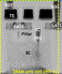
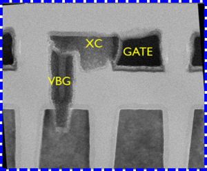
And when transistors can’t be made any smaller, the only way to make progress is to go upwards.