Design challenge

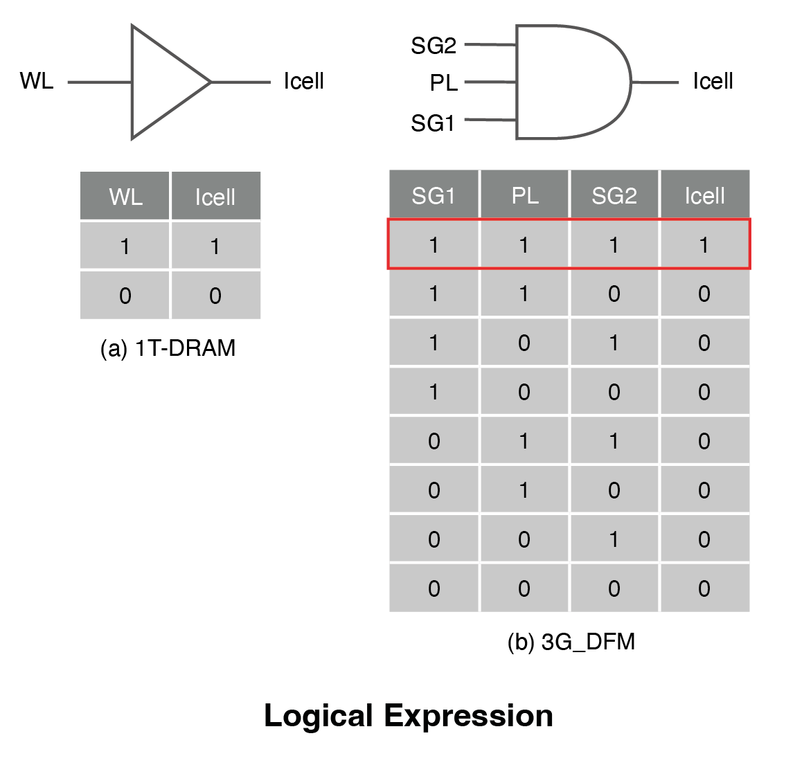
Main memory is implemented in Dynamic RAM (DRAM), which provides a better trade-off between density and access times compared with Static RAM (SRAM). The density advantage of DRAM is due to its use of one transistor and one capacitor (1T1C) to store a single bit, in contrast to SRAM, which uses up to 6 transistors to store a single bit.

However, with the charge stored on the capacitor, reading the bit cell drains the capacitor (a destructive read), requiring the bit to be written back – and if the DRAM is not read, the charge will eventually leak out of the capacitor anyway. For this reason, DRAM bit cells must be periodically refreshed. Regular refresh cycles are power hungry and reduce read/write bandwidth.

The scaling of DRAM to improve density is coming to an end, as capacitors do not shrink as well as transistors. It is difficult to build a capacitor in a small cell area with enough capacitance, leading to short data retention, insufficient sensing margin and interference. It also increases power consumption due to greater leakage currents by shortening the refresh cycle.

DRAM vendors are currently grappling with the scaling, power and cost walls while planning a transition beyond a cell size of 6F2 – dealing with both capacitor aspect ratio and capacitive coupling. Meanwhile customers demand ever-increasing amounts of external memory, while also expecting a decline in bit cost.

Stacked DFM: how it works

Stacked Dynamic Flash Memory (DFM) is a capacitor-less DRAM alternative/supplement to traditional 1T1C DRAM, the workhorse memory of the industry. It works by exploiting the ‘floating body effect’. It is composed of a single transistor with two or three gates. The Plate Line PL gate acts as a memory device, and gates SG1 and SG2 act as switching gates. Also, two or three gates can be composed of double gates, and one of the two gates is grounded, so that the stored holes are undisturbed.

It is programmed with “1” by source-side impact ionization, generating hole-electron pairs. During this the PL and SG2 gates operate in the linear region with the virtual drain of the inversion layer below PL and SG2, while the SG1 gate operates in the saturation region. The source-side impact ionization is used similarly to a Flash memory programming mechanism. But a much smaller electric field is needed for hole generation by the impact ionization in comparison with Flash memory, so unlike Flash memory, no reliability problems occur.

DFM-1

A “0” erase occurs when positive voltages are applied to PL, SG2 and BL. Unlike earlier 1T DRAM implementations, no negative voltage is applied to the BL or SL, so no negative charge pump or twin-well process are required, reducing power and layout area. Also, this erasure scheme with only positive voltages, can significantly relax the GIDL (Gate Induced Drain Leakage) current, which may destroy the stored data – which occurred in Z-RAM.

DFM-2

The three gates together ensure a large margin between “1” and “0”, reduce capacitive coupling, provide a robust disturbance shield from the Bit Line BL and Source Line SL and thereby increase retention time – without increasing silicon area.

Previous attempts to develop DRAM without capacitors have been unsuccessful, as seen in Z-RAM where the margins between “1” and “0” were too narrow.

In DFM the Plate Line PL gate eliminates the floating body, and with a significant increase in the “1” and “0” margin results in noticeably increased speeds and improvements in the reliability of the memory cell. It does this by using the PL (Plate Line) gate to ‘stabilize’ the floating body and by separating “1” write and “0” erase modes, allows for the widest possible margin – avoiding issues with noise and the fluctuation of the floating body.

Hole Concentration After “1” Write (PL = 0V, 85°C)

Reads are non-destructive. By omitting the capacitor, DFM leaks more slowly than 1T1C DRAM. The DFM has not only page erase and page refresh but also block erase and block refresh, akin to flash. The latter improves refresh duty cycle, i.e., the time spent doing refresh.

In order to lower bit cost – an industry imperative – DFM has the potential to be stacked vertically or horizontally.

DFM-7
diagram-4.3f-two-stack-DFM

When implementing 2 tiers of three gate (3G) Stacked DFM (14F2), it is equivalent to 1T1C DRAM (~6F2 ), and when implementing just 4 to 8 tiers, it is equivalent to a 4 to 2F2 cell size – requiring fewer tiers than 3D Stacked 1T1C DRAM. It should be noted that the common technology for 3D Stacked 1T1C DRAM fabrication can also be utilized for Stacked DFM.

diagram-4.3i-DFM-cell-size-and-stacks

Benefits

Stacked DFM is ideal as a dense DRAM alternative or supplement:

  • Significant bit cost (Gb/mm2) improvements over DRAM
  • It can be stacked either horizontally or vertically, without the capacitor issues that will complicate 3D DRAM stacking, where capacitors are flipped on their side, greatly increasing area
  • Large margin and robust against disturbance
  • Low leakage current, thanks to the absence of a capacitor and fewer leakage paths
  • Power efficient operation, thanks to very low leakage and non-destructive reads, reducing the frequency and overhead of refresh cycles – and freeing additional bandwidth for normal reads and writes. Block refresh and block erase further improve performance