In an era where Dennard scaling is over and Moore’s Law is maturing, semiconductor design and fabrication requires engineers to address four interrelated challenges together, specifically the:
Architecture follows application

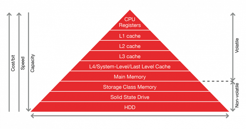
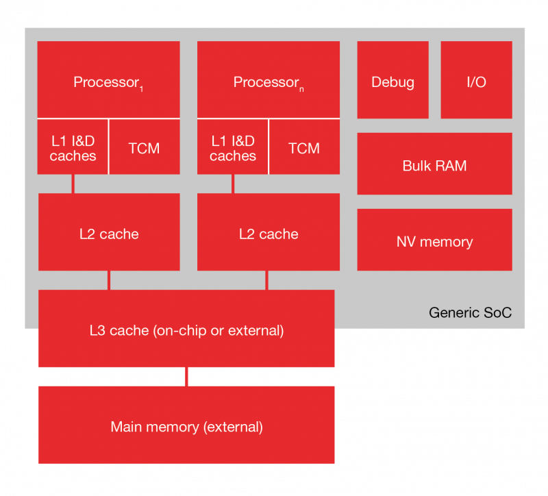
In the memory-storage hierarchy of a modern System-on-Chip (SoC), embedded SRAM (eSRAM) is typically used to implement on-chip L1 and L2 caches, and optionally, Tightly Coupled Memories (TCM) – the latter used for deterministic, or predictable, access times (as caches are inherently non-
deterministic).

A L3, system level (SLC) or last level cache (LLC), may also be present. Depending on the target application, and cost & design constraints, this may be on-chip or external (perhaps implemented via a chiplet), and may be implemented in SRAM or DRAM.
There may also be embedded bulk RAM present, as a low-latency on-chip memory, as well as some non-volatile (NV) memory.
External DRAM is used as main memory.
This configuration has come under pressure due to an explosion in dataset sizes – especially with AI/ML at the edge – and an increase in processor performance across a range of both applications and SoC price points.
This means the amount of memory required has greatly increased, as has the gap between processor performance and memory performance.
While embedding memory on-chip brings memory closer to the processor, improving bandwidth and hiding latency, the demand for memory means that there will still be a requirement for external main memory – and that it too will increase.
But the four walls continue to cast a shadow.
Embedding on-chip DRAM or SRAM faces issues largely related to the scaling and power walls, specifically density, stability and leakage.
Using external DRAM increases system power consumption due to off-chip memory accesses, and bandwidth is limited by the inflexible external memory interface, decided – just like supply and pricing strategies – by a small number of external DRAM companies, potentially affecting SoC system
performance, system cost and device lifetime.
And external DRAM scaling is likewise reaching a limit.
When you need it both ways
So, you need to support a big increase in the amount of both embedded and external memory.
And you cannot afford to greatly increase silicon area, or device and overall system cost.
Unisantis Electronics has developed two memory technologies to respond to this challenge – Dynamic Flash Memory (DFM) and Key-shaped Floating Body Memory (KFBM).
We have also developed the Surrounding Gate Transistor (SGT), a vertical Gate-All-Around (GAA) FET, which is ideal for ultra-low power designs for both logic and memory such as SRAM.


